Research Interests
Research Interests
| ★ High Density Data Storage The explosive increase in information and the miniaturization of electronic devices demand new recording technologies and materials that combine high density, fast response, long retention time, and rewriting capability. Among the various recording media for ultrahigh density data storage, organic materials have attracted many attentions for their low cost, simplicity, good stimuli-responsive properties, and versatility in molecular design. From the structure and function of materials, a series of organic functional thin films were prepared as information storage media, which could write, erase and rewrite nanoscale information dots. The results provide new approaches for the design of erasable ultrahigh density information storage materials. A stable organic material (N,N′-dimethyl-N′(3-nitrobenzylidene)-p-phenylene-diamine (DMNBPDA)) with a strong electron donor –N(CH3)2, and an electron acceptor –NO2 was synthesized. By applying proper pulsed voltages between the STM tip and the substrate, information dots with diameter of about 1.1 nm was achieved successfully (Adv. Mater. 2003, 15, 1525-1529); Based on intermolecular hydrogen bonds and π-π interaction,,single crystal films were prepared via self-assembly. recording dots with the average diameter of 2.2 nm and the spacing of 1 nm were realized (Adv. Mater. 2004, 16, 2018-2021); through the structure design of materials, erasable 3D high density optical information storage (Adv. Mater. 2005, 17, 156-160) and high signal to noise ratio optical memory (Chem. Mater. 2006, 18, 235-237) were achieved; utilizing strong electron donor-accepter molecules with rigid structure, the self-assembled film for ultra high density information storage was prepared by vacuum deposition (Adv. Mater. 2005, 17, 2170-2173). To further study the relationship between the structure and photoelectric properties of material, the photoelectric dual high density information storage with the same material was demonstrated (ChemPhysChem 2005, 6, 478-482). Base on the enhancement effect of 3D photonic crystals on the fluorescence, high performance optical information storage was developed (Adv. Mater. 2010, 22, 90-94) Recently, the film of a new charge transfer molecule was prepared, which exhibited reversible control of appearing and hiding of information dots (J. Mater. Chem., 2012, 22, 4299-4305, cover). To further improve the density of individual storage devices, multi-level memory device was demonstrated by using the synergistic effect of photo-electronic switch of a meta-conjugated donor-bridge-acceptor molecule (J. Am. Chem. Soc. 2012, 134, 20053 - 20059).
|
|
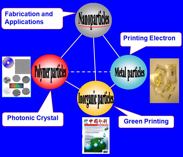
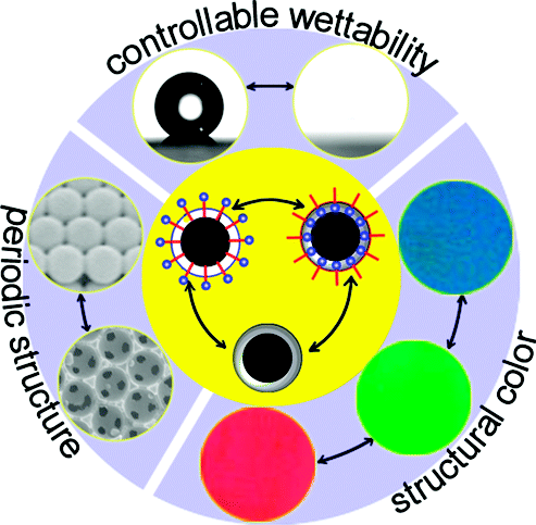
| ★ Fabrication and Applications of Photonic Crystals Because of the regulation performance of photon propagation, photonic crystal material is called "optical semiconductor", which has caused intensive attention. We focused on the preparation and applications of photonic crystals (Acc. Chem. Res. 2011, 44, 405-415; J. Mater.Chem. 2011, 21, 14113-14126). Based on structure design, latex particles with hard core and soft shell structure were prepared, which were assembled to photonic crystals with close packed structure and high strength (Macromol. Chem. Phys. 2006, 6, 596-604), as well as controllable wettability (Chem. Mater. 2006, 18, 4984-4986; Adv. Funct. Mater. 2007, 17, 219-225) The slow photon effect of 3D photonic crystals and its enhancement effect on the fluorescence was demonstrated (J. Mater. Chem. 2007, 17, 1237-1241). The photonic crystals were used for high sensitivity detection (Angew. Chem. Int. Ed. 2008, 47, 7258-7262; J. Mater. Chem. 2012, 22, 21405-21411), optical information storage, (Adv. Mater. 2010, 22, 1237-1241) etc.. Through the control of latex particle morphology, the wettability and adhesion could be controlled (Adv. Funct. Mater. 2011, 21, 4436-4441), and photonic crystals with ultra narrow band gap was prepared based on the modulation of interfacial properties (J. Am. Chem. Soc. 2012, 134, 17053-17058; NPG Asia Mater.2012,4,e21) Furthermore, the photonic crystals were used in high performance solar cell concentrator, light catalysis and so on (J. Mater. Chem. 2008, 18, 2650-2652; Energ. Environ. Sci. 2010, 3, 1503-1506). The polymer latex particles also could be used in inkjet printing technology (J. Mater. Chem., 2009, 19, 5499 - 5502), which allowed the dyes pigment was instead of the structure color, and provided new materials and solutions to environmental friendly printing technology (J. Mater. Chem. C. 2013,DOI: 10.1039/C3TC30728J). Printed photonic crystal detection chips and their applications were further developed (Lab Chip 2012, 12, 3089-3095;J. Mater. Chem.2012, 22, 21405-21411). Based on the difference of substrate wettability, the photonic crystal chip with multi band gap array was designed and fabricated, and the photonic crystal chip could efficiently detect and identify multi substrate (Angew. Chem. In. Ed. 2013, 52, 7296-7299). |
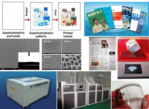
| ★ Green Printing Materials and Technologies Printing industry is one of the backbone industries in China. The mainstream plate-making technology in China is Laser Typesetting, and Computer-To-Plate. Both technologies are based on the photosensitizing process. Therefore they inevitably include complex processes, which cause problems of high cost, and serious pollution. Through the long-time and in-depth research with nano materials and printing science (Chem. Soc. Rev. 2013, 42, 5184-5209; Adv. Mater. 2013, 25, 2291-2295), a kind of non-photosensitive, non-pollution, and inexpensive nanometer green plate making technology is developed and the environmental pollution in the process of plate making is expected to be solved completely. So far, the green printing technology has been broken through in critical materials, high speed and high precision green plate making equipment, as well as the bundled software, and more than 50 patents were applied or granted. We further developed environment friendly plate-base technique as well, and the huge environmental pollution and energy consumption in the traditional electrolytic oxidation process could be solved completely. The water-based ink for plastic gravure printing has been developed via enterprise cooperation and also realized industrialization. The green printing technology has been extended to printing electronics, printing and dyeing textiles, Printing and patterning of building materials and so on. It is expected that completely green printing industry technical chain will be developed based the innovation of nano-materials.
|